Wave Soldering Explained: Process, Applications & Common Defects
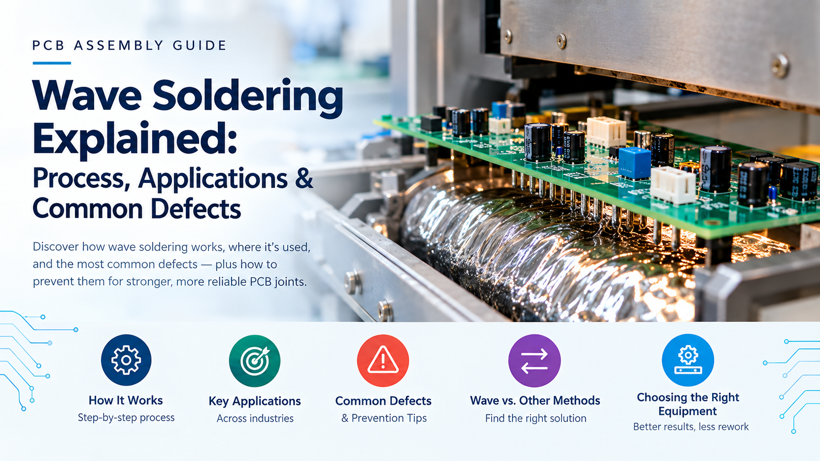
Wave Soldering Explained: Process, Applications & Common Defects
Wave soldering remains one of the most reliable and cost-effective methods for soldering through-hole components onto printed circuit boards (PCBs) at scale. Despite the rise of surface mount technology (SMT), wave soldering continues to play a critical role in mixed-technology assemblies, connectors, and high-current components that demand strong mechanical and electrical joints.
What Is Wave Soldering?
Wave soldering is an automated PCB assembly process in which a board is passed over a continuously flowing "wave" of molten solder. As the board moves across the wave, solder adheres to the exposed metal pads and component leads on the underside of the board, creating strong, reliable solder joints in a single pass.
The Wave Soldering Process, Step by Step
- Fluxing: The board first passes over a flux station, where flux is applied to the exposed copper areas to remove oxidation and promote solder adhesion.
- Preheating: Before reaching the solder wave, the board is gradually preheated to activate the flux, drive off solvents, and reduce thermal shock when it contacts the molten solder.
- Solder Wave Contact: The preheated board passes over one or two waves of molten solder — typically a turbulent wave for penetration followed by a smoother laminar wave to minimize bridging and icicles.
- Cooling: After exiting the solder wave, the board cools gradually, allowing the solder joints to solidify properly and reducing the risk of fractured or dull joints.
- Inspection & Cleaning: Depending on the flux type, boards may be cleaned and inspected using AOI or manual inspection.
Common Applications of Wave Soldering
- Power supply units and industrial power electronics
- Automotive electronics
- Consumer electronics with mixed-technology boards
- Telecommunications and networking equipment
- High-reliability and industrial control systems
Common Wave Soldering Defects and How to Prevent Them
| Defect | Typical Cause | Prevention |
|---|---|---|
| Bridging | Excess solder, incorrect wave height, tight component spacing, or contaminated flux | Optimize wave height and conveyor angle, review PCB pad spacing, and use clean, properly activated flux. |
| Insufficient wetting / dry joints | Poor flux activation, inadequate preheating, oxidized or contaminated leads, or solder pot temperature that's too low | Verify the preheat profile, use fresh and properly activated flux, and confirm solder pot temperature is within spec. |
| Icicles | Low solder temperature, excess flux, or a conveyor exit angle that's too shallow | Adjust solder pot temperature and conveyor exit angle, and control flux volume. |
| Voids in plated through-holes | Inadequate preheating, insufficient wave dwell time, or a board thickness-to-hole-diameter ratio that limits solder flow | Adjust wave turbulence and dwell time, and check the board's thickness-to-hole-diameter ratio during design review. |
Wave Soldering vs. Other Soldering Methods
Manufacturers often weigh wave soldering against reflow and selective soldering. Reflow soldering is the standard for SMT components and offers tighter control for fine-pitch parts, but it isn't suited to through-hole leads. Selective soldering targets individual through-hole joints on boards that mix SMT and through-hole components, making it well suited to low-volume or high-mix production, though it's slower per board than wave soldering. Wave soldering remains the most efficient choice for boards with a high density of through-hole components at medium-to-high production volumes. In practice, mixed-technology assemblies often combine these processes depending on component type and production requirements.
Choosing the Right Wave Soldering Equipment
Getting consistent, defect-free results from wave soldering depends heavily on equipment quality, including preheat zone control, wave height stability, and nitrogen atmosphere options. Working with a supplier that understands both the equipment and process parameters can help reduce defect rates and rework costs.
Looking to Upgrade Your PCB Assembly Line?
Leaptech supplies and supports wave soldering and complete PCB assembly automation solutions for manufacturers across India. Get in touch with our team to discuss the right setup for your production requirements.