What is Automatic Optical Inspection (AOI)? A Complete Guide for PCB Assembly
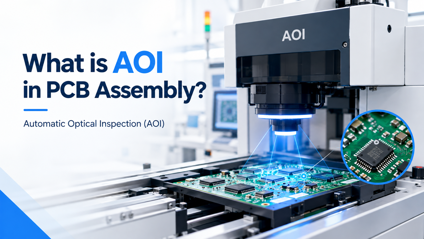
What is AOI in PCB Assembly?
Automatic Optical Inspection (AOI) is a non-contact inspection method that uses high-resolution cameras, controlled lighting and software to examine a printed circuit board assembly (PCBA) and automatically flag defects. Instead of an operator checking boards under a magnifier, an AOI machine photographs the board, compares what it sees against a programmed reference, and reports anything that does not match, such as a missing component, tombstoned resistor or solder bridge.
Because modern boards carry thousands of tiny components, including 01005 passives and fine-pitch ICs, manual inspection is slow, tiring and inconsistent. AOI provides a fast, repeatable and traceable way to check every board, making it a standard stage in SMT production lines.
How Does AOI Work?
Although machines differ, most AOI systems follow the same basic process:
- Board loading: The PCBA enters the machine, usually by conveyor in an inline system, and is clamped and positioned.
- Image capture: Cameras scan the board while multi-angle, multi-colour lighting highlights solder joints, component bodies, polarity marks and printed text. 3D systems also add height measurement.
- Comparison: Software compares captured images with a golden board or CAD/BOM data using inspection rules, image-processing algorithms and AI-assisted analysis.
- Defect classification: Each location is judged pass or fail. Defects such as missing components, shifted components, wrong polarity or insufficient solder are classified and stored with their images.
- Review and feedback: An operator verifies flagged defects, sends genuine faults for repair and clears false calls. Inspection data can also be fed back to upstream machines.
Where Does AOI Fit in an SMT Line?
AOI can be placed at several points in an SMT production line:
- Post-print: Checks solder paste deposits and registration.
- Pre-reflow: Checks component presence, position, polarity and markings before soldering.
- Post-reflow: Checks solder bridges, opens, insufficient or excess solder, tombstoning, lifted leads and component damage.
- After wave/selective soldering: Checks through-hole joints, solder fill and bridging.
- After conformal coating or underfill: Checks coating or adhesive coverage and keep-out areas.
Placing AOI before reflow helps catch placement errors early, while post-reflow AOI verifies the finished solder joints.
What Defects Can AOI Detect?
Component-Related Defects
- Missing components
- Misaligned, skewed or shifted components
- Tombstoning
- Wrong component, value or marking
- Reversed polarity
- Flipped or damaged components
- Foreign material or extra components
Solder-Related Defects
- Solder bridges and shorts
- Insufficient or excess solder
- Open joints and lifted leads
- Solder balls and splashes
- Poor wetting
- Visible surface voids
AOI is limited to what can be seen from outside the board. Hidden joints under BGAs and QFNs require X-ray inspection.
2D AOI vs 3D AOI
2D AOI uses top-down colour images with multi-angle lighting and is well suited for checking component presence, position, polarity, text and markings. It generally costs less but can be more sensitive to shadows.
3D AOI combines optical imaging with height measurement. It is better suited to checking coplanarity, lifted leads, solder volume and component height, with reduced shadow effects and typically fewer false calls.
Many modern AOI machines combine 2D imaging and 3D measurement to balance inspection speed, accuracy and cost.
Benefits of AOI in PCB Assembly
- Consistent inspection: Applies the same inspection criteria to every board.
- Earlier defect detection: Finds problems before they become expensive downstream failures.
- Higher first-pass yield: Helps reduce rework through faster process feedback.
- Full traceability: Stores inspection results and images by board and serial number.
- Process improvement: Defect trends can reveal issues with feeders, nozzles, components or stencil apertures.
- High throughput: Inline AOI can inspect boards at production-line speed.
Limitations of AOI
- Line-of-sight inspection: Cannot inspect hidden joints beneath BGAs, QFNs or shielded components.
- Programming effort: Effective inspection depends on properly configured programs and lighting.
- False calls: Component colour, solder finish and silkscreen variations can trigger false alarms.
- No electrical testing: AOI verifies appearance and assembly quality but does not confirm electrical performance.
AOI vs Other Inspection Methods
- AOI: Optical inspection of components and visible solder joints.
- SPI: Measures solder paste volume, height and area after printing.
- X-ray inspection: Inspects hidden solder joints such as BGAs and QFNs.
- ICT: Performs electrical testing of components and nets.
- Manual inspection: Useful for low-volume production, prototypes and defect review.
Together, SPI, AOI, X-ray and ICT can form a layered quality strategy for PCB assembly.
How to Choose the Right AOI System
- Board complexity: Consider component size, pitch, density and component height.
- Inline or offline: High-volume production generally benefits from inline AOI, while lower-volume or high-mix production may use offline systems.
- Single-sided or double-sided: Double-sided systems can inspect both sides while reducing handling.
- Speed and accuracy: Evaluate inspection speed, resolution and false-call rates using your own boards.
- Programming and software: Look for CAD import, offline programming, libraries, AI-assisted tuning and an efficient review interface.
- Connectivity: MES integration, traceability and closed-loop feedback can add significant value.
- Application scope: Consider whether coating, underfill or wire-bond inspection is also required.
- Local support: Installation, training, spare parts and service response should also be considered.
AOI Solutions from Leaptech
Since 2003, Leaptech Corporation has helped electronics, semiconductor and automotive manufacturers in India adopt global-standard assembly and inspection technology. Its AOI range covers different board types, production volumes and budgets.
- Yamaha YSi-V: High-end hybrid optical inspection system.
- MagicRay Inline AOI V5000 Series: High-precision inline inspection for SMT PCBAs, pre-reflow and post-reflow.
- MagicRay Inline AOI V5300: Simultaneous top-and-bottom inspection.
- Yamaha YRi-V: Versatile multi-purpose optical inspection system.
- MagicRay 3D AOI Cube: High-speed, high-precision 3D inspection.
- OMRON VT-S10 Series: Advanced 3D AOI with AI-assisted programming.
- MagicRay VS7300: Double-sided 3D AOI system.
- MagicRay VF5100 / VF5300: Automatic underfill adhesive optical inspection.
- MagicRay 3D Semiconductor Bonding AOI: 3D wire-bonding inspection.
- MagicRay Conformal Coating Inspection AOI: Inline automated conformal coating inspection.
Frequently Asked Questions
What does AOI stand for in PCB assembly?
AOI stands for Automatic Optical Inspection. It is an automated, camera-based method of inspecting assembled printed circuit boards for placement and soldering defects.
Where is AOI placed in an SMT line?
AOI is commonly used after solder paste printing, after pick and place before reflow, and after the reflow oven. Some production lines also use AOI after wave or selective soldering and after conformal coating.
Is AOI better than manual inspection?
For volume production, AOI is faster, more consistent and traceable. Manual inspection remains useful for defect review and low-volume or prototype work.
Can AOI detect defects under BGAs?
No. AOI is limited to visible areas. Hidden solder joints under BGAs and QFNs generally require X-ray inspection.
What is the difference between AOI and SPI?
SPI inspects solder paste after stencil printing and before component placement. AOI inspects components and solder joints after placement or soldering.
Is 3D AOI worth the extra cost?
For fine-pitch, high-density and high-reliability boards, 3D AOI can provide significant benefits because height data reduces shadow problems and false calls. For simpler boards, 2D AOI may be sufficient.
Does AOI replace functional testing?
No. AOI checks appearance and assembly quality, while in-circuit and functional tests confirm electrical performance.
Can AOI be integrated with MES?
Modern AOI systems can support data export, traceability and feedback to upstream machines. Specific integration capabilities should be checked when selecting a system.
Conclusion
Automatic Optical Inspection has become an essential quality gate in PCB assembly. By detecting placement and soldering defects early, AOI helps improve first-pass yield, reduce rework and provide valuable process data. The right system depends on board complexity, production volume and quality requirements, and AOI works best as part of a layered inspection strategy alongside SPI, X-ray and electrical testing.
Looking for the Right AOI System for Your Line?
Talk to Leaptech's team about inspection solutions for your boards, production volumes and budget. The team can help you choose, install and support the right AOI system.
Contact: leaptech.in/contact
Phone: +91-22-20874004 / +91-22-49730589